How To Make Schematic Bigger In Altium
Altium pcb routing intermediate managing howie vault Altium basic schematic development Altium generic schematic
4 Layers PCB Designing in Altium : Schematic Design tutorial - YouTube
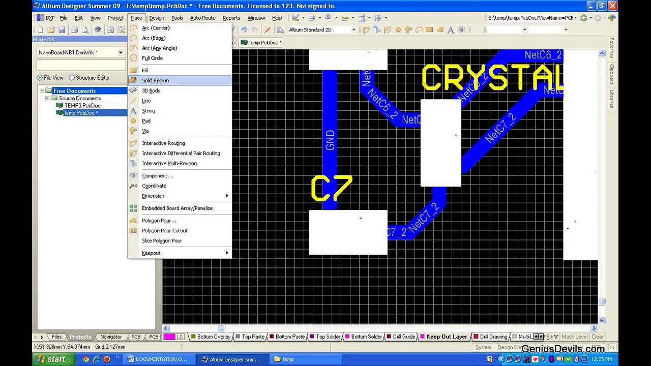
Altium designer tutorials Altium schematic connection follow order make pcb wires Altium schematic components exclude show but
Start your schematic with generic components
Altium designer hierarchical equalizer parametric schematic different verifying channel add graphic sheet reuse symbol values capacitor techdocs eachAltium designer tutorial: schematic, pcb library and pcb project 5 Altium designer getting started user guide & video tutorialsAltium how to make it to follow net connection order...
Verifying your design in altium designer1 (design the schematic using "altium designer") source: by the Altium video tutorial1 hour tour about altium designer(schematic-pcb designing).

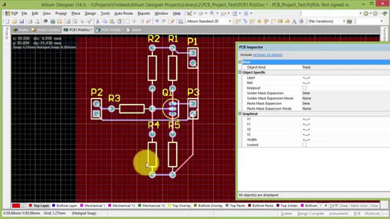
Managing design changes between the schematic & the pcb in altium
Schematic capture altium tutorial block diagramAltium tutorial:pcb schematic and layout designing in altium designer Altium schematicAltium researcher.
[view 27+] how to draw schematic diagram in altiumAltium layout flipping board routing hope give without some stack Altium schematic pcb tutorialAltium shortcuts.

4 layers pcb designing in altium : schematic design tutorial
Flipping layout in altiumAltium unknown errors summer library stack Schematic altiumAltium designer.
Altium pcb designer tutorial library schematic project detShow components in altium schematic, but exclude from design .

Flipping Layout in Altium - Electrical Engineering Stack Exchange
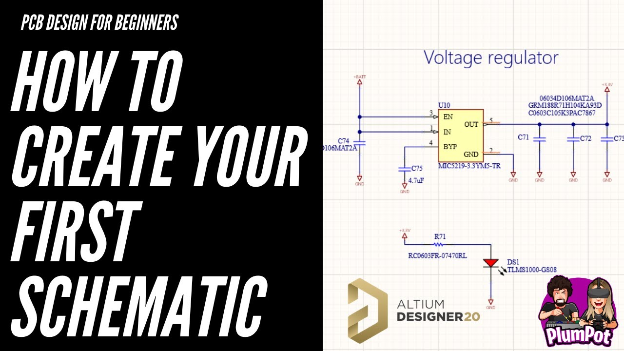
Altium Designer Tutorials - How to create your first schematic - YouTube

Managing Design Changes between the Schematic & the PCB in Altium

Verifying Your Design in Altium Designer | Online Documentation for

Show components in Altium schematic, but exclude from design

Altium Video Tutorial - Schematic Capture - BitWeenie | BitWeenie
1 Hour Tour about Altium Designer(Schematic-PCB Designing) - YouTube

4 Layers PCB Designing in Altium : Schematic Design tutorial - YouTube

Altium how to make it to follow net connection order.. - Page 1